(MENAFN- Asia Times) Like a steel-eyed gambler in Las Vegas, Beijing is doubling down on its bet.
But they''re not playing for a pot of cash, the prize is bigger, much, much bigger.
And no nation, on this planet of ours, plays the long game better than China.
As the US recently proposed a stricter policy to ban exports to China of semiconductor manufacturing equipment, it's full speed ahead on designing and building high-end chipsets within the mainland.
Digitimes reports that Huawei will build its first wafer fabrication manufacturing company in Wuhan, Hubei Province. According to the information, the company is expected to start production in stages from next year.
Sources reveal that this factory initially used to produce optical communication Kirin chips and modules to gain self-sufficiency and keep a good quantity of required chipsets.
Digitimes further claims that this factory will be used to produce optical communication chips and modules to gain self-sufficiency and create microcircuit designs.
As we all know, HiSilicon, Huawei's chip designing subsidiary has the capability to design advanced chip designs.
And while Huawei is best known for its telecom equipment dominance, currently the company's Wuhan-based Research Institute has nearly 10,0000 R & D personnel that mainly research and develop optical communication equipment, HiSilicon chips and even automotive laser radars.
In fact, HiSilicon might be the only company in China that has the ability to develop a coherent optical DSP chipset.
In the proposed plan, Huawei will back the Wuhan HiSilicon factory project with a total of CNY 1.8 billion investment.
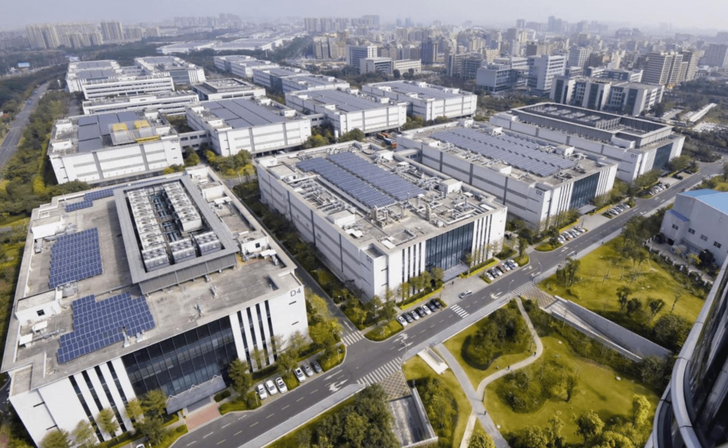
Currently, Huawei's Wuhan-based Research Institute has nearly 10,0000 research and development personnel that mainly researching and developing optical communication equipment, HiSilicon chips, and automotive laser radars. Credit: Handout.
It's mission — develop its own chipset for smartphones and other IoT devices.
And how is that possible, with China trailing Taiwan and South Korea, in advanced chipset design?
According to an industry insider who spoke to Asia Times, you don''t need to put a 5 nm chip into a laptop because processing is moving back to the center with rapid emergence of 5G.
The key is fast communications, which means, the Chromebook idea could dominate the market in the future.
''You can set up massive parallel processing arrays with 14-28 nm chips that are as fast as you want, and the laptop is simply a dumb terminal for this central processor,'' the insider said.
''The importance of the superfast, narrow gateway chips is exaggerated. China can now or soon will be able to produce all the 14-28 nm chips it needs — and that's 98-99% of the total market.''
China's 30-year-long semiconductor journey has grown into a major player, accounting for nearly 13% of the global IC design market in 2020.
Amid the continuing trade and tech standoff with the US, China has been speeding up the development of domestic fabrication plants to localize the most vital elements of the technology supply chain.
In that IC assembly line, a lithography machine is fundamental to the entire manufacturing chain.
China's ''national champion'' in the area, Shanghai Micro Electronics Equipment (SMEE), which was founded in 2002 by Shanghai Electric Group, is, per some reports, full speed ahead to develop its second-generation deep ultraviolet (DUV) immersion lithography system, which could produce down to 7nm chips with multiple patterning.
In 2002, a lithography machine technology research project was first included in China's National High-tech R & D Program (863 Program). SMEE was founded in the same year.
Its research in the area continued in the ''02 Special Project,'' along with other 15 National Special Projects published in the National Outlines for Medium and Long-term Planning for Scientific and Technological Development (2006-2020) in 2006.
The 02 Special Project focuses on the extensive circuit integration and peripheral equipment manufacturing, where developing a home-grown lithography machine supply chain was one of the critical tasks.
Since the project was launched, SMEE has gradually become the primary designer and the ''integrator'' of a plethora of made-in-China lithography equipment components.
By no means, is this a magic carpet ride — China's chip industry still faces massive challenges and fierce competition.
But to date, SMEE has developed 4 series of lithography machines for IC front-end manufacturing, IC back-end advanced packaging, LED/ MEMS/power devices and TFT circuit manufacturing.
As of June 2021, SMEE's most advanced device is its ''600 series'' scanner for IC front-end manufacturing. This machine can be used to build chips at the 90nm, 110nm and 280nm process technologies.
Meanwhile, Huawei is yet to make any official announcement or confirmation on the HiSilicon factory in Wuhan.
''It's very unlikely that the US will remove us from the Entity List,'' billionaire founder Ren Zhengfei said in February at the opening of a mining innovation laboratory partly sponsored by Huawei. ''Right now, we just want to work harder and keep looking for new opportunities to survive.''
Sources: Huawei Central, Equal Ocean, Digitimes, MySmartPrice, Al Jazeera, Bloomberg
MENAFN27062021000159011032ID1102352105
Legal Disclaimer:
MENAFN provides the information “as is” without warranty of any kind. We do not accept any responsibility or liability for the accuracy, content, images, videos, licenses, completeness, legality, or reliability of the information contained in this article. If you have any complaints or copyright issues related to this article, kindly contact the provider above.