IEEE Study Leverages Silicon Photonics For Scalable And Sustainable AI Hardware
"While silicon photonics are easy to manufacture, they are difficult to scale for complex integrated circuits. Our device platform can be used as the building blocks for photonic accelerators with far greater energy efficiency and scalability than the current state-of-the-art", explains Dr. Tossoun.
The team used a heterogeneous integration approach to fabricate the hardware. This included the use of silicon photonics along with III-V compound semiconductors that functionally integrate lasers and optical amplifiers to reduce optical losses and improve scalability.
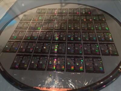
The fabrication started with silicon-on-insulator (SOI) wafers that have a 400 nm-thick silicon layer. Lithography and dry etching were followed by doping for metal oxide semiconductor capacitor (MOSCAP) devices and avalanche photodiodes (APDs). Next, selective growth of silicon and germanium was performed to form absorption, charge, and multiplication layers of the APD. III-V compound semiconductors (such as InP or GaAs) were then integrated onto the silicon platform using die-to-wafer bonding. A thin gate oxide layer (Al2O3 or HfO2) was added to improve device efficiency, and finally a thick dielectric layer was deposited for encapsulation and thermal stability.
This unique photonic platform can achieve wafer-scale integration of all of the various devices required to build an optical neural network on one single photonic chip, including active devices such as on-chip lasers and amplifiers, high-speed photodetectors, energy-efficient modulators, and non-volatile phase shifters. Going forward, the photonic platform will enable datacenters to accommodate more AI workloads and help solve several optimization problems.
The platform will be addressing computational and energy challenges, paving the way for robust and sustainable AI accelerator hardware in the future!
Reference
Title of original paper: Large-Scale Integrated Photonic Device Platform for Energy-Efficient AI/ML Accelerators
Journal: IEEE Journal of Selected Topics in Quantum Electronics
DOI: 10.1109/JSTQE.2025.3527904
Media Contact:
Kristen Amoroso
+1(732) 562-6694
[email protected]
SOURCE IEEE Photonics Society

Legal Disclaimer:
MENAFN provides the
information “as is” without warranty of any kind. We do not accept
any responsibility or liability for the accuracy, content, images,
videos, licenses, completeness, legality, or reliability of the information
contained in this article. If you have any complaints or copyright
issues related to this article, kindly contact the provider above.
Most popular stories
Market Reseach
- B2PRIME Strengthens Institutional Team's Growth With Appointment Of Lee Shmuel Goldfarb, Formerly Of Edgewater Markets
- BTCC Exchange Scores Big In TOKEN2049 With Interactive Basketball Booth And Viral Mascot Nakamon
- Ares Joins The Borderless.Xyz Network, Expanding Stablecoin Coverage Across South And Central America
- Primexbt Launches Stock Trading On Metatrader 5
- Solana's First Meta DEX Aggregator Titan Soft-Launches Platform
- Moonacy Protocol Will Sponsor And Participate In Blockchain Life 2025 In Dubai
- Primexbt Launches Instant Crypto-To-USD Exchange


Comments
No comment