(MENAFN- Asia Times) The US Commerce Department's Bureau of Industry and Security (BIS) last week moved Chinese NAND flash memory maker Yangtze Memory Technologies Co (YMTC) from its“Unverified List” to its“Entity List”, the Biden administration's latest punitive move against a major Chinese technology company.
In the words of the BIS, those who qualify for the Entity List“have been involved, are involved, or pose a significant risk of being or becoming involved in activities contrary to the national security or foreign policy of the United States.”
Sales of semiconductor production equipment, electronic design automation software and other products to YMTC will now be subject to“stringent license requirements” that cover exports not only from the US but of products made in other countries using US technology.
Entities on the Commerce Department's Unverified List are subject to export restrictions until the BIS either verifies their bona fides or decides to move them to the Entities List. YMTC was added to the Unverified List last October.
NAND flash is one of the two main types of semiconductor memory; the other is DRAM. Invented by Toshiba engineer Fujio Masuoka in 1987, it is now used in memory cards, USB drives, solid state drives (SSDs), personal computers, servers, data centers and cell phones.
NAND flash memory chips are a high-tech, high-volume commodity. Most of them are made by Samsung Electronics and SK hynix of South Korea, Japan's Kioxia (formerly part of Toshiba) and Micron Technology of the US. American chipmaker Intel agreed to sell its NAND flash business to SK hynix in 2020.
NAND flash chips were originally single-layer, but in order to achieve higher storage capacity, several chips were stacked in the same package. Then, in 2013, Samsung introduced the first 3D NAND, which had 24 layers of storage cells on one chip. The entire industry took the same route, introducing 32-, 64-, 96- and 128-layer devices one after another.
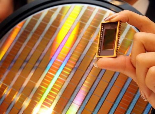
An employee of Samsung Electronics shows a 30-nanometer 64-gigabit NAND flash memory device. Photo: AFP / Kim Jae-hwan
As a newcomer to the industry, YMTC skipped this transition. Founded in Wuhan in 2016, it started with 32-layer 3D NAND and burst upon the scene two years later when it introduced its patented“Xtacking” architecture and a 64-layer device at the Flash Memory Summit held in Santa Clara, California, in 2018. For this, it received one of two awards for Most Innovative Flash Memory Start-up Company.
Xtacking is a unique architecture in which the logic circuits that handle data transfer and other peripheral circuitry are built on one silicon wafer, which is then bonded to a second wafer holding the memory storage cells. YMTC claims that this reduces product development time and shortens the manufacturing cycle while permitting smaller die size and higher bit density.
Other companies fabricate 3D NAND on single wafers. In 2020, YMTC launched commercial 64-layer 3D NAND products and announced that it had developed 128-layer technology. In September 2021, the integrated circuit teardown experts at TechInsights found 128-layer 3D NAND from YMTC in an Asgard Memory SSD, indicating that the Chinese company had almost caught up with the rest of the industry.
Some outside observers believe that Xtacking is an unsustainably expensive approach that will require ongoing subsidies from the Chinese government. Earlier this month, industry analyst Jim Handy of Objective Analysis told EE Times:“I have always wondered how something built on two wafers can compete against something with the same die size built on a single wafer. Given that YMTC doesn't need to be profitable, that may work for a while.”
Not surprisingly, YMTC vice president of research and development Hongbin Zhu has a different view. Delivering a keynote address at the 2022 Flash Memory Summit held in August, he said that Xtacking is now mass production capable and cost competitive, has good performance and is reliable, and that it is an extendable platform for future innovation. Xtacking 3.0, the latest version of the architecture, received one of ten awards for Most Innovative Memory Technology.
Zhu has spent more than 20 years in semiconductor R&D with a focus on process, equipment and materials development, and process integration. He holds a PhD in chemical engineering from the University of Arizona and more than 100 patents. His presentation can be viewed here .
In October 2021, Xperi Holding Corp, which advertises itself as“an American technology company that licenses technology and intellectual property in areas such as mobile computing, communications, memory and data storage, and three-dimensional integrated circuit technologies, among others,” licensed its“foundational portfolio” of semiconductor bonding technology to YMTC.
This technology, according to Xperi,“...is a key enabling technology for current and future generations of high performance, high-capacity 3D NAND flash memory.”
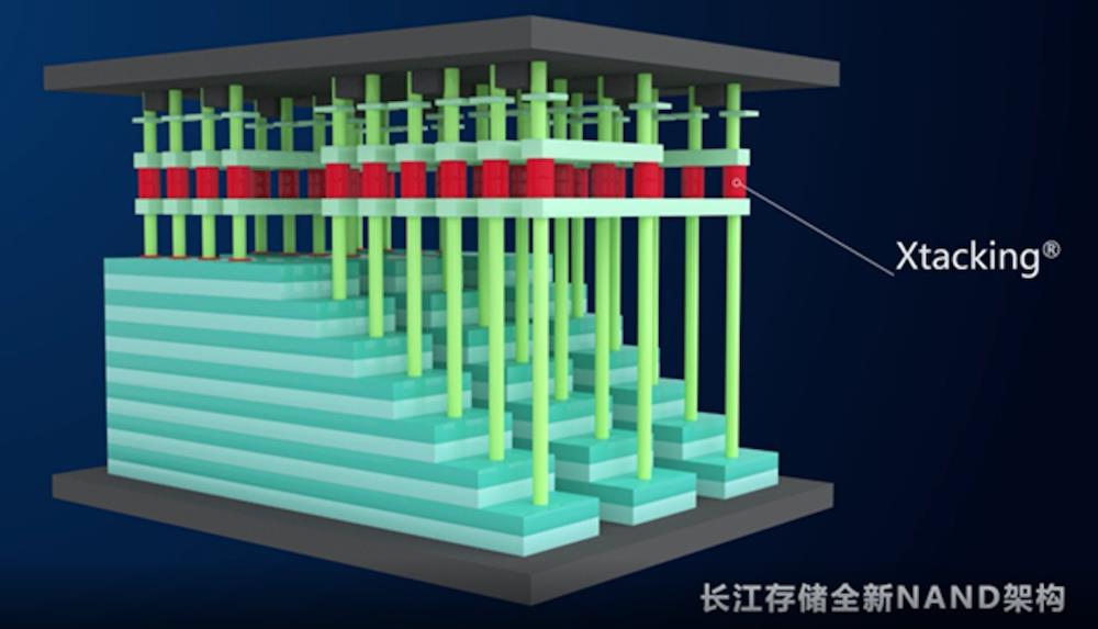
YMTC's patented“Xtacking” NAND chipmaking technique. Image: Twitter / TechInsights
Specifically, it“enables the disaggregation of the memory array and logic circuitry allowing the optimal wafer process node to be used for each.” Which is to say, it is ideally suited to YMTC's Xtacking architecture.
In March 2022, it was reported that Apple was evaluating YMTC's 3D NAND flash memory for possible use in iPhones sold in China. It was also reported that YMTC was offering prices 20% lower than those of its competitors. By October, its 128-layer devices had reportedly been certified but not yet used in production.
In November, TechInsights found Xtacking 232-layer 3D NAND flash memory in an SSD from Hikvision, which was put on the Entity List in 2019. According to TechInsights, this was“the first 200+ layer 3D NAND Flash solution on the market, putting YMTC ahead of Samsung, Micron [and others]... And although the (now former) market leaders are all working at the 200+ layer generation, YTMC is the first we've seen in production.”
TechInsights was duly impressed:“What YMTC has accomplished has been nothing short of amazing. Not only have they leap-frogged the biggest semiconductor companies in the world, but they did also it despite being headquartered in Wuhan, often facing crippling lockdowns during a worldwide pandemic. So, although the chips might seem to be stacked against them given today's geo-political challenges, they certainly shouldn't be ruled out.”
However, China-bashing politicians in the US were outraged. In September, the office of Senator Marco Rubio issued a statement saying:
“ Earlier this month, Apple publicly acknowledged that it is considering procuring NAND memory chips for future iPhones from Yangtze Memory Technologies Co. (YMTC), a state-owned company with extensive links to the Chinese Communist Party (CCP) and its armed wing, the People's Liberation Army (PLA).
“US Senators Marco Rubio (R-FL) and Mark Warner (D-VA), vice chairman and chairman of the US Senate Select Committee on Intelligence, sent a letter to US director of National Intelligence Avril Haines calling for a public analysis and review of YMTC and the risks it presents to US national security. Majority Leader Chuck Schumer (D-NY) and Senator John Cornyn (R-TX) also signed the letter.”
After YMTC was put on the Unverified List in early October, Apple dropped its plans to source 3D NAND from YMTC.
Last week, when it became apparent that YMTC would be placed on the Entity List, Schumer said,“The Biden administration needed to act swiftly to prevent YMTC from gaining even an inch of a military or economic advantage.”
Semiconductor industry analysts estimate that YMTC now has about 5% of the NAND flash memory market, with some of them earlier predicting it would soon come to dominate the market.
Now some of them are writing that YMTC will be crippled by sanctions, with the company likely to find it difficult to operate without US-made equipment and probably impossible in future to license more US technology.
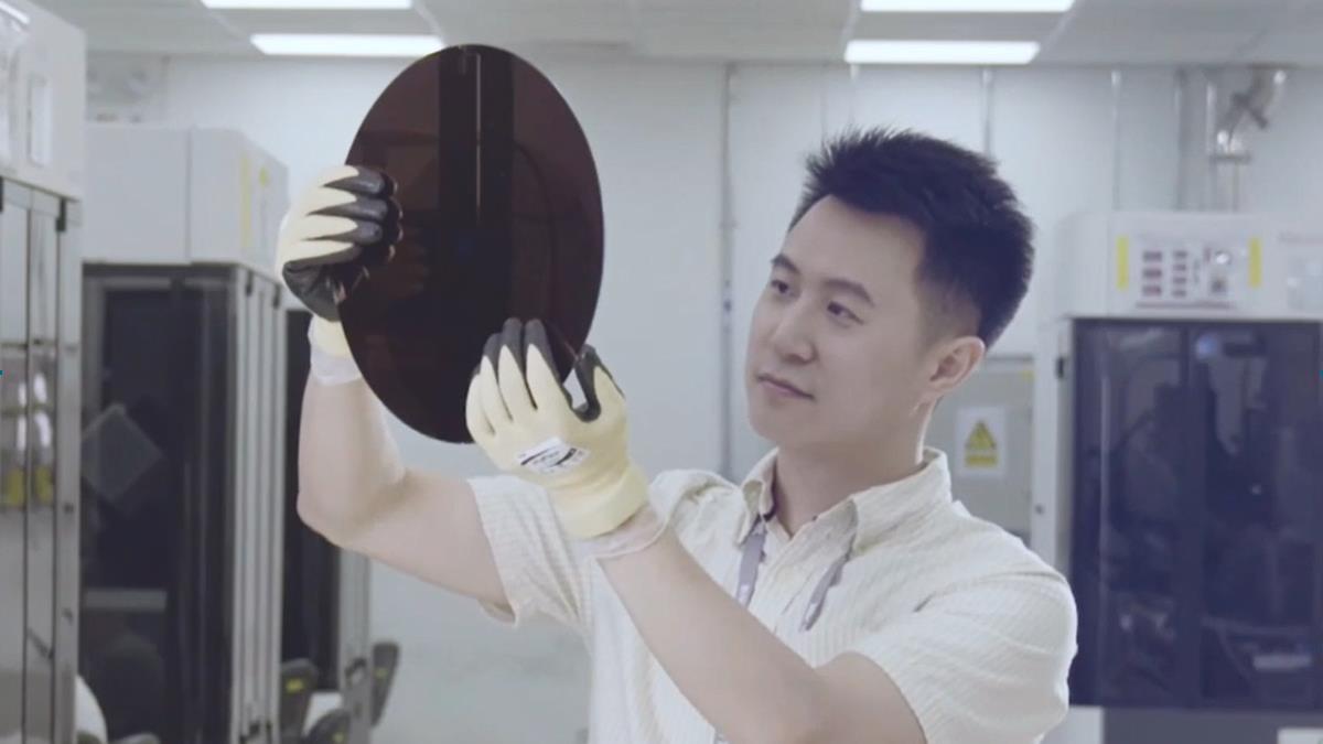
A YMTC worker examines a semiconductor wafer before the company was put on a US 'Entity List'. Photo: YMTC
Significantly, Entity List restrictions cover 128-layer 3D NAND. YMTC already has it in production, apparently at a volume and quality acceptable to Apple, but will find it more difficult to produce without support from etch equipment maker Lam Research, inspection equipment maker KLA and other US suppliers.
Ramping up production of Xtacking 232-layer chips is likely to be delayed long enough for YMTC's competitors to fend off the challenge.
Micron, which announced mass production of 232-layer NAND flash memory last July, is now advertising what it claims to be the world's first SSD incorporating that device. Samsung started mass production of 236-layer chips in November. SK hynix plans to launch a 238-layer device next year. Kioxia aims to introduce a 200+ layer device in 2024.
All these companies have vastly greater production capacity than YMTC, no problem buying the latest chip-making equipment and the ability to develop their own version of Xtacking if that should prove to be the most efficient way to produce future generations of 3D NAND flash memory.
On the other hand, the Chinese market for NAND flash memory is large and the Chinese government will help YMTC take full advantage of it. Having lost Apple as a customer, the company will turn to Xiaomi and other Chinese smartphone makers, which account for more than a third of the global market. Whatever YMTC can make, it can likely sell in China.
The next Flash Memory Summit is scheduled for August 2023. It will be interesting to see if YMTC participates and if it does, what its representatives will have to say after being placed on the Entity List.
Follow this writer on Twitter: @ScottFo83517667




Comments
No comment