


403
Sorry!!
Error! We're sorry, but the page you were looking for doesn't exist.
Semiconductor Inspection Microscope Market Size To Hit USD 10.98 Billion By 2033 Research By SNS Insider
| Report Attributes | Details |
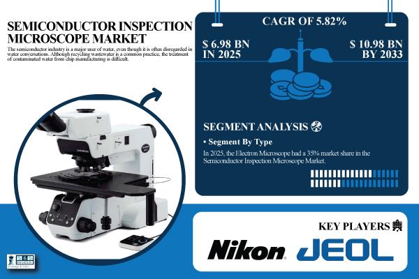
| Market Size in 2025 | USD 6.98 Billion |
| Market Size by 2033 | USD 10.98 Billion |
| CAGR | CAGR of 5.82% From 2026 to 2033 |
| Report Scope & Coverage | Market Size, Segments Analysis, Competitive Landscape, Regional Analysis, DROC & SWOT Analysis, Forecast Outlook |
| Key Segmentation | . By Type (Electron Microscope, Scanning Probe Microscope, Optical Microscopes & Others) . By Components (Software, Hardware & Services) . By Application (Transistors, Memory Blocks, Interconnection Devices Integrated Circuits & Others) |
Purchase Single User PDF of Semiconductor Inspection Microscope Market Report (20% Discount) @
Difficulty in Examining Tiny Semiconductor Structures May Hinder Market Expansion Globally
Light diffraction limits the ability of conventional optical microscopes to identify features smaller than 200 nanometers. Defect identification is made more difficult by the sophisticated 3D structures of contemporary chips. Effective manufacturing requires striking a compromise between fast throughput and high-resolution inspection, but doing so is currently quite difficult. Production productivity is impacted since a SEM analysis of a wafer can take minutes, but an inspection may only take seconds.
Key Industry Segmentation
By Type
In 2025, the Electron Microscope had a 35% market share in the Semiconductor Inspection Microscope Market. The electron microscopes, specifically Scanning Electron Microscopes (SEMs), are commonly utilized in semiconductor examination due to their high resolution and capability to visualize both the exterior and interior features of semiconductor devices.
By Components
Based on Component, Hardware dominated the Semiconductor Inspection Microscope Market with 45% of share in 2025. The microscope hardware, such as the optical system, illumination system, and stage, controls the market because of its high cost and complexity.
By Application
Integrated circuits lead the market due to their growing complexity, which makes defect detection more challenging. Semiconductor inspection microscopes are crucial for examining integrated circuits for defects, such as scratches, cracks, and particles, ensuring they meet quality standards and perform reliably.
Regional Insights:
North America is witnessing growing adoption of semiconductor inspection microscopes driven by increasing use of AI and machine learning to detect defects with greater precision. The presence of major chip manufacturers and advanced research institutions is boosting demand for ultra-high-resolution inspection systems.
Asia Pacific continues to dominate the market due to rapid semiconductor manufacturing expansion in China, Taiwan, South Korea, and Japan. Growing investments in EUV lithography and advanced nodes are pushing demand for extremely accurate inspection microscopes.
Do y ou h ave a ny s pecific q ueries o r n eed a ny c ustomiz ed r esearch on Semiconductor Inspection Microscope Market ? Submit your inquiry here @
Recent Developments:
- In Sep 2025 – KLA Corporation launched new AI-centric semiconductor process-control solutions enabling nanoscale defect detection for advanced GPU, HBM, and heterogeneous chip architectures to support next-generation AI manufacturing. In September 2025 - Onto Innovation Showcases Advanced Metrology & Inspection Solutions at SEMICON West 2025, driving leadership in AI and next-gen semiconductor packaging.
Exclusive Sections of the Semiconductor Inspection Microscope Market Report (The USPs):
- PRICING & COST BENCHMARKS – helps you understand the average price trends across optical, electron, and scanning probe microscope types, with insights into regional cost variations and feature-based pricing (AI-assisted or 3D inspection), supporting strategic procurement and investment decisions. USAGE & PERFORMANCE METRICS – enables you to assess operational efficiency through data such as average wafers inspected per day, defect detection accuracy, and device downtime, assisting fabs and foundries in benchmarking productivity and reliability. TECHNOLOGICAL ADOPTION RATE – highlights the penetration of AI/ML-based inspection, 3D imaging, and MES-integrated systems, helping identify innovation leaders and track the shift toward intelligent semiconductor inspection solutions. APPLICATION & INDUSTRY UTILIZATION INDEX – provides insights into adoption trends across semiconductor types (logic, memory, power devices) and emerging applications like AI chips and photonics, offering visibility into market diversification and growth potential. REGULATORY & COMPLIANCE INSIGHTS – helps you evaluate the percentage of devices meeting ISO/SEMI standards, cleanroom certifications, and energy compliance, ensuring alignment with global manufacturing and environmental norms. R&D AND INNOVATION TRENDS – tracks ongoing investment in next-gen imaging technologies, revealing the innovation intensity among leading microscope manufacturers and uncovering opportunities for collaboration or technology adoption.
About Us:
SNS Insider is one of the leading market research and consulting agencies that dominates the market research industry globally. Our company's aim is to give clients the knowledge they require in order to function in changing circumstances. In order to give you current, accurate market data, consumer insights, and opinions so that you can make decisions with confidence, we employ a variety of techniques, including surveys, video talks, and focus groups around the world.
CONTACT: Contact Us: Rohan Jadhav - Principal Consultant Phone: +1-315 636 4242 (US) | +44- 20 3290 5010 (UK)
Legal Disclaimer:
MENAFN provides the
information “as is” without warranty of any kind. We do not accept
any responsibility or liability for the accuracy, content, images,
videos, licenses, completeness, legality, or reliability of the information
contained in this article. If you have any complaints or copyright
issues related to this article, kindly contact the provider above.
Most popular stories
Market Research

More Story


Comments
No comment