


403
Sorry!!
Error! We're sorry, but the page you were looking for doesn't exist.

Japan On Edge Of EUV Lithography Chip-Making Revolution
(MENAFN- Asia Times)
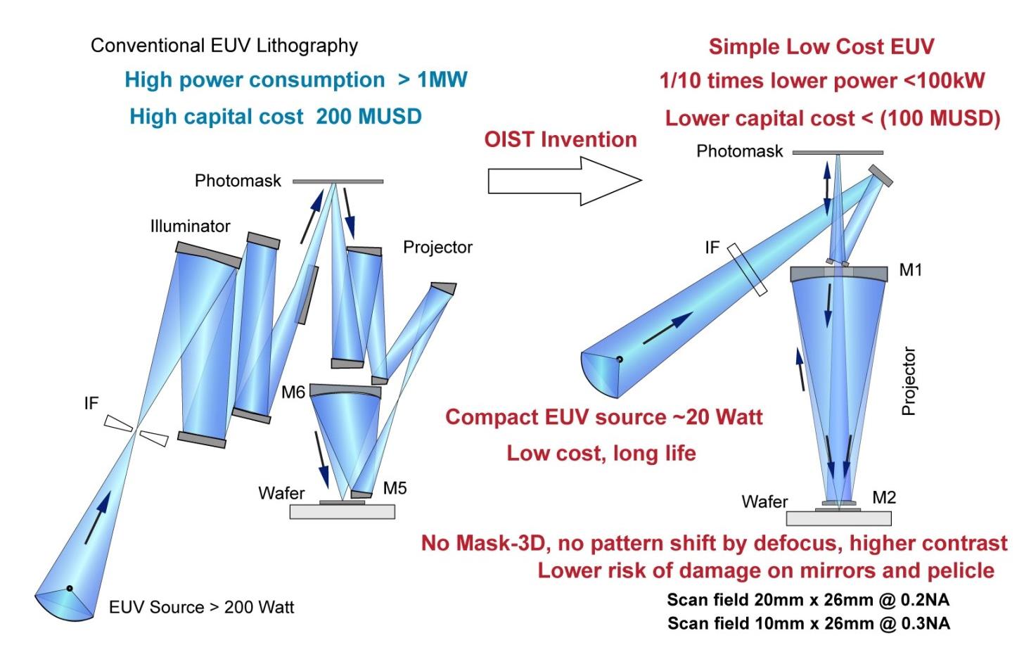
The Okinawa Institute of Science and Technology (OIST) has designed a new type of extreme ultraviolet (EUV) lithography equipment that could significantly reduce the cost to produce 7nm and smaller semiconductors, and thus revolutionize the chip manufacturing supply chain.
![]()
OIST's Tsumoru Shintake. Image: OIST
According to reports, the EUV equipment's optical system is greatly simplified while power consumption is reduced by a factor of ten, raising the prospect of much cheaper advanced chip-making machines.
If so, it could mark the end of ASML's monopoly on EUV lithography, which would have serious implications for semiconductor manufacturers, investors and governments.
Recall that US sanctions forbid the sale of EUV lithography equipment to China, making it much more difficult and expensive for Chinese companies to make semiconductors at 7nm and 5nm, and impossible at the 3nm node now in production at Taiwan's TSMC and the 2nm and smaller nodes currently under development.
AI processors, the low-power semiconductor devices used in smartphones, and the latest high-density memory chips are made using highly complex EUV lithography equipment that is expensive to maintain and consumes enormous amounts of power.
OIST Professor Tsumoru Shintake says the invention is a breakthrough technology that can nearly completely solve these problems.
OIST's Tsumoru Shintake. Image: OIST

Legal Disclaimer:
MENAFN provides the
information “as is” without warranty of any kind. We do not accept
any responsibility or liability for the accuracy, content, images,
videos, licenses, completeness, legality, or reliability of the information
contained in this article. If you have any complaints or copyright
issues related to this article, kindly contact the provider above.
Most popular stories
Market Research

More Story


Comments
No comment