Centura Sculpta Chip-Making Tool Puts China Further Behind
Announced on February 28, the Centura Sculpta should make it possible to reduce the number of EUV (extreme ultraviolet) lithography steps used to manufacture integrated circuits at the most advanced process nodes, significantly reducing both complexity and cost.
US sanctions already ban the export of EUV lithography tools to China. Without them, 7nm and 5nm processes are not economical and 3nm, 2nm and smaller processes cannot be implemented at all.
As efficiency gains drive the adoption of EUV, China is likely to be left farther behind in the race to develop next-generation chips for smartphones, artificial intelligence, quantum computing and other high-tech industries.
This, however, does not mean the end of the Chinese semiconductor industry. As Asia Times' David Goldman points out,“Older-generation 28nm chips power most of Huawei's digital infrastructure and industrial applications, and China can produce those itself.”
Factories and logistics controlled by 5G networks are where China's comparative advantage now lies, Goldman consistently argues.
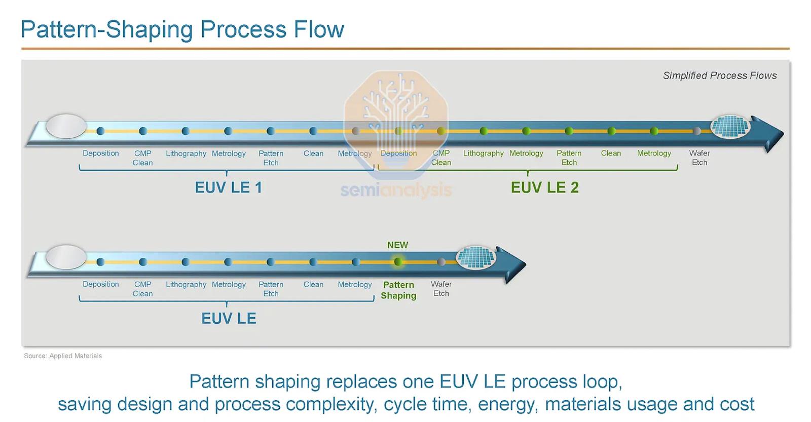
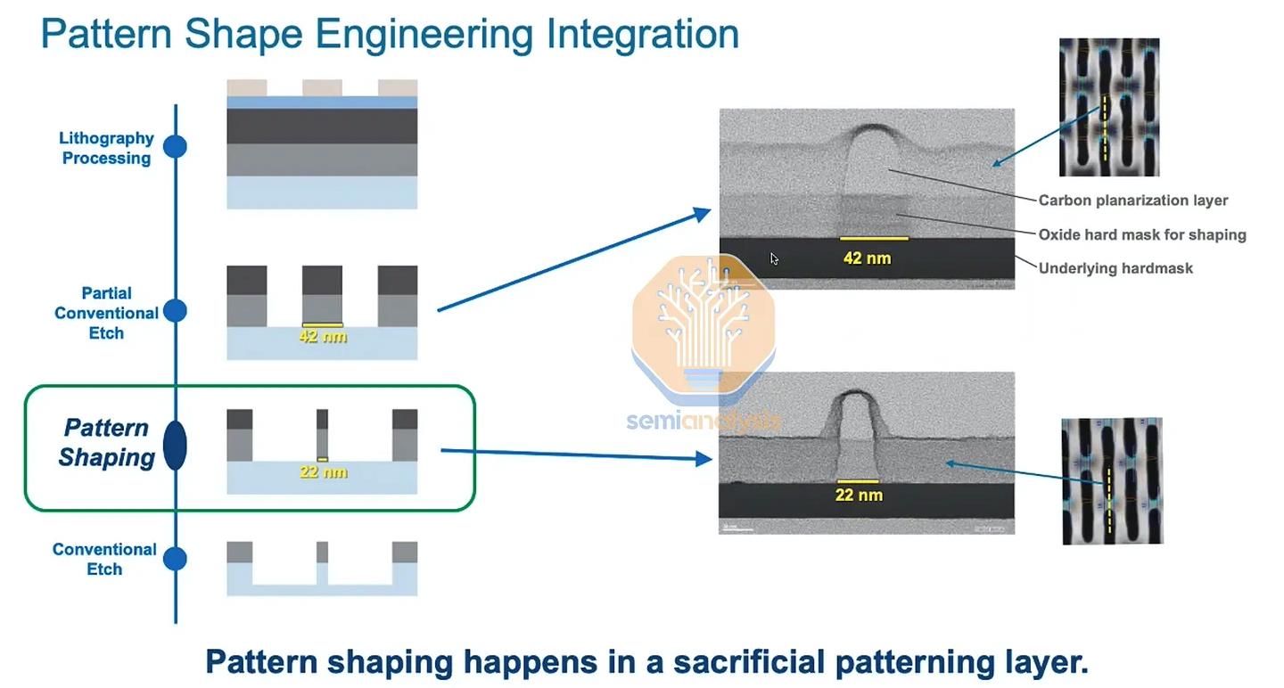
Sculpta is a sophisticated etching tool that uses a beam of plasma to modify the dimensions of chip features on the silicon wafer, reducing the need for double or multiple patterning.
In order to print feature sizes smaller than the resolution limit of current EUV lithography (13nm), circuit patterns are split in two, each half conforming to the resolution limit; the halves are then combined to produce a finer and denser pattern.
This double patterning requires a“litho-etch-litho-etch” (LELE) process that takes more time and uses additional equipment, materials and energy. Multiple patterning repeats this process. In this way, feature sizes have been greatly reduced but at an ever-increasing cost.
Sculpta offers an alternative to this escalation.“Sculpta is intended for the most critical patterning layers in advanced logic nodes,” says Applied Materials.“Because the final pattern is created from a single mask, design cost and complexity are reduced, and the yield risk from double-patterning alignment errors is eliminated.”

Graphic: Applied Materials
The potential cost savings are enormous. Applied Materials claims that for each EUV double patterning sequence it replaces, Sculpta enables:
- a reduction in capital costs of about US$250 million per 100K wafer starts per month of production capacity;
- manufacturing cost savings of approximately $50 per wafer; and
- significant reductions in energy consumption, use of water and emission of greenhouse gases.
To put all this in perspective, leading chipmaker TSMC is reported to have raised its 5nm production capacity to 150,000 wafers per month.
EUV lithography tools now cost almost $170 million each and ASML's next-generation high-NA (numerical aperture) tools may cost twice as much. High-NA will bring the resolution limit down to 8nm, reducing the need for multiple patterning – but not immediately; the first machines are not scheduled for delivery until 2024.
In the meantime, lithography accounts for an estimated 35% of the cost of production at 3nm. ASML, of the Netherlands, currently has a monopoly on EUV lithography.
Applied Materials claims that Sculpta pattern shaping could cut the use of EUV lithography by half for some critical layers, while semiconductor industry analysts estimate that it could reduce total unit demand for EUV lithography tools by nearly 20%.
Estimates are rough because it is not yet known how quickly Sculpta might be adopted, whether or not it will live up to expectations and what impact the cost savings might have on semiconductor-making capacity expansion plans.
Sculpta is a new product but pattern shaping is not a new technology, which tips the scales in favor of its success. Applied Materials has been issuing research papers about it for several years and market research organizations report that Intel may introduce it at 1.8nm in 2024 or 2025 (although it could come much sooner). Samsung is expected to be the second user and TSMC the third, most likely at 1.4nm according to industry observers.

Image: Applied Materials
Ryan Russell, a corporate vice president at Intel, says,“Having collaborated closely with Applied Materials in the optimization of Sculpta around our process architecture, Intel will be deploying pattern-shaping capabilities to help us deliver reduced design and manufacturing costs, process cycle times and environmental impact.”
Dan Hutcheson, a highly regarded analyst of semiconductor industry trends now at TechInsights, says,“Sculpta is the most innovative new process step in wafer fabrication since the introduction of CMP.”
CMP (chemical mechanical planarization), which is used to remove excess material and create a smooth wafer surface, is one of several steps in the manufacturing process – in addition to EUV lithography – that will be affected by the introduction of Sculpta.
Others include photomask making and inspection; photoresist deposition and removal; and materials deposition, etch and cleaning.
Companies whose order flow is likely to be affected include ASML (the Netherlands), Applied Materials itself and Lam Research (USA), Tokyo Electron, JSR, Hoya and Lasertec (Japan), and many others. Etch equipment makers Lam Research and Tokyo Electron will be pressed to introduce their own versions of pattern shaping.
It is tempting to conclude that the only beneficiary will be Applied Materials and its customers but that is not necessarily the case. The semiconductor industry is driven by efficiency gains and cost reduction, and Sculpta has the potential to accelerate progress toward the 1nm process node.

China is doubling down on its indigenous chip-making capabilities but it may be falling further behind. Image: Twitter
Pattern shaping could help Intel catch up with TSMC and Samsung and thereby speed up the growth of the EUV lithography market. It could lead to a quicker and greater return on JSR's acquisition of metal-oxide photoresist maker inpria , which is aimed at 1nm.
On the other hand, fewer EUV masks would reduce demand for Hoya's mask blanks and Lasertec's mask inspection tools.
None of the companies directly affected is Chinese. But the entire Chinese semiconductor industry is once again reminded that the leading edge is a moving target and being etched outside of its borders.
Follow this writer on Twitter: @ScottFo83517667

Legal Disclaimer:
MENAFN provides the information “as is” without warranty of any kind. We do not accept any responsibility or liability for the accuracy, content, images, videos, licenses, completeness, legality, or reliability of the information contained in this article. If you have any complaints or copyright issues related to this article, kindly contact the provider above.


Comments
No comment