Scanning atoms with the tip of a needle

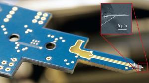
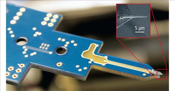
The improved cantilever of Dr. Ruppert

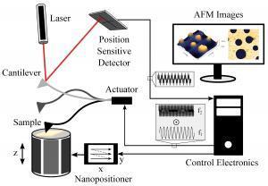
Schematic setup of a traditional multifrequency atomic force microscopy experiment. A cantilever vibrates at multiple resonance frequencies simultaneously while it is being scanned over a sample by a nanopositioner.

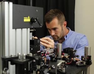
Dr. Michael Ruppert aligning a custom active cantilever in a modified atomic force microscope.
Digitizer from Spectrum helps researchers to improve the Atomic Force Microscope
The Spectrum unit allows us to make simultaneous high-resolution, low-noise measurements of multiple integrated sensor regions in order to correctly characterize our system's performance. — Dr. Michael RuppertGROSSHANSDORF, GERMANY, February 24, 2021 /EINPresswire.com / -- The Atomic Force Microscope (AFM) is an important tool in materials science and used for mechanical scanning of surfaces. The forces acting between the atoms of the surface and the tip of a nanoscopic needle are measured and calculated giving resolutions in the order of fractions of a nanometer. Now, the University of Newcastle in Australia is improving and simplifying these complex machines, so that a wider use in laboratories worldwide will be possible. In this sophisticated research, an 8-channel Spectrum digitizerNETBOX provides the high precision needed to push the evolution of AFMs.The Atomic Force Microscope (AFM), invented in 1985, became a vital tool used by laboratories around the world that are involved in surface chemistry. Its outstanding resolution means that this instrument can reveal more detail than conventional light-based microscopes by a factor of more than 1000 times. And, unlike other advanced systems such as electron microscopes, it can image samples in situ. This, along with the ability to perform topographical imaging and force measurements, makes AFMs well suited for the study of soft biological materials, polymers, nanostructures and various other materials.
At the University of Newcastle, Dr. Michael Ruppert and his team are improving the key elements of AFM systems. The aim is to simplify the operation as well as to enhance the overall performance of these microscopes. The Precision Mechatronics Lab at the University's School of Electrical Engineering and Computing brings together expertise in nanotechnology, mechatronics, microelectromechanical systems (MEMS) and low-noise electronic design to create unique solutions that can reduce an AFM's system complexity and cost.
An AFM typically creates a topographical image by scanning a cantilever/tip across a sample surface. A laser beam and position-sensitive photodiode detector is then used to determine small changes in cantilever deflection. Signals from the detector need to be acquired and analyzed in order to determine any topological height changes on the sample's surface to create a three-dimensional topography.
At the core of the instrument is a microcantilever which interacts with the sample and provides the 'physical link' to measuring nanomechanical properties. While cantilever microfabrication technology has continuously advanced over the years, the overall design has remained largely unchanged; a passive rectangular cantilever has been adopted as the industry wide standard. Consequently, conventional cantilever instrumentation requires external piezo-acoustic excitation as well as an external optical deflection sensor. Both of these components are not optimal for trends in multifrequency AFM technology which can extend the imaging information beyond the topography to a range of nano-mechanical properties including sample stiffness, elasticity and adhesiveness. In contrast, active cantilevers with integrated actuation and sensing on the chip level provide several distinct advantages over conventional cantilever including the absence of structural modes of the mounting system, the possibility of down-scaling, single-chip AFM implementations, parallelization to cantilever arrays as well as the absence of optical interference.
Dr. Ruppert and his co-workers have recently published a number of papers that propose novel, integrated cantilever designs to improve AFM performance, simplify operation and drastically reduce the footprint and equipment costs. The papers discuss topics that include innovative cantilever designs to optimize deflection sensitivity, achieve arbitrary placement of resonance frequencies and allow integrated robust multimode Q control. In collaboration with the University of Texas at Dallas, Dr. Ruppert also co-developed the first silicon-on-insulator, single-chip, MEMS AFM that features integrated in-plane electrostatic actuators and electrothermal sensors, as well as an AlN piezoelectric layer for out-of-plane actuation and integrated deflection sensing. The approach has the potential to significantly reduce the cost and complexity of the AFM and expand its utility beyond current applications.
To undertake this type of research, it is important to have high precision measuring equipment that allows the acquisition and analysis of the sensor signals from these integrated microcantilevers. By determining the amplitude noise spectral density, important parameters of the cantilever system can be obtained including the thermal noise at resonance, the cantilever tracking bandwidth, and the electronic noise floor of the instrumentation. For this purpose, the research group uses a model DN2.593-08 digitizerNETBOX from Spectrum Instrumentation . The unit has eight fully synchronized digitizer channels each capable of sampling signals at rates up to 40 MS/s with 16-bit resolution. For control and data transfer, the digitizerNETBOX connects to a host computer via a simple Gbit Ethernet cable.
Researcher Dr. Michael Ruppert says: "Having a measuring tool like the digitizerNETBOX is essential for the work we are doing here at the Precision Mechatronics Lab. The unit allows us to make simultaneous high-resolution, low-noise measurements of multiple integrated sensor regions in order to correctly characterize our system's performance."
About Spectrum Instrumentation
Spectrum Instrumentation, founded in 1989, uses modular design to create a wide range of digitizers and generator products as PC-cards (PCIe and PXIe) and stand-alone Ethernet units (LXI). In 30 years, Spectrum has gained customers all around the world, including many A-brand industry-leaders and practically all prestigious universities. The company is headquartered near Hamburg, Germany, and known for its outstanding support that comes directly from the design engineers. More information about Spectrum can be found at
Sven Harnisch
Spectrum Instrumentation
+49 4102 69560
email us here

Legal Disclaimer:
MENAFN provides the
information “as is” without warranty of any kind. We do not accept
any responsibility or liability for the accuracy, content, images,
videos, licenses, completeness, legality, or reliability of the information
contained in this article. If you have any complaints or copyright
issues related to this article, kindly contact the provider above.


Comments
No comment