(MENAFN- Asia Times) Tokyo Electron (TEL) expects a sharp drop in sales of semiconductor-making gear in the second half of this fiscal year, a downturn that will be deepened and prolonged by new US sanctions on exporting advanced chips and related production equipment to China.
TEL, one of Japan's largest electronics and semiconductor private companies, has cut its sales guidance for the six months to March 2023 by more than 25%, reminding those who follow the semiconductor industry – and those politicians who think they can manage it – that demand can turn on a dime and that the industry is still highly cyclical.
President Toshiki Kawai told analysts and the media that about half of the reduction in anticipated sales, amounting to an estimated 250 billion yen (US$1.8 billion), owes to the impact of US sanctions on China's semiconductor industry, a the company flagged in early August.
Kawai also said that TEL will not take advantage of the sanctions to win new orders in China at the expense of American competitors subject to US Commerce Department's export restrictions. Those competitors include Applied Materials and Lam Research, both of which have said the sanctions will have a significant negative impact on their business.
The other driving force behind TEL's downward sales revision is a broad industry downturn that started last quarter. Intel, Micron, SK hynix and TSMC have already announced large reductions in capital spending. Samsung has announced smaller but still material cuts. All of these companies – and most other integrated circuit (IC) makers – are TEL customers.
TEL expects sales to memory IC makers to drop by 40% in the second half of this fiscal year, while sales to logic IC makers, including foundries, to fall by 10%. In October, TSMC CEO C C Wei told the media,“We expect probably in 2023 the semiconductor industry will likely .”
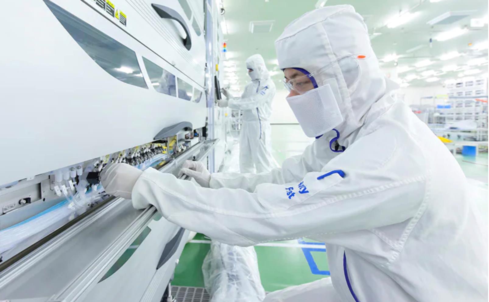
Tokyo Electron expects sales to decline into 2023. Image: TEL website
TEL cut its second-half operating profit guidance by more than 50%, largely due to high gearing to changes in sales but also to high parts and materials costs and rising deprecation and R&D spending. Net profit guidance for the second half of the fiscal year was slashed by 44%.
For the full year to March 2023, TEL is now forecasting a 4.8% increase in sales, 8.9% decline in operating profit and 8.5% fall in net profit. Previous guidance was for increases of 17.3%, 19.5% and 19.7%.
TEL's results for the six months to September and new guidance for the year to March next year were announced after the market closed on November 10. The next day, the company's share price jumped 8.4% as part of a market rally sparked by lower inflation in the US. TEL shares are still down 36% from an all-time high reached in December 2021 but have since rebounded by 28% from their 52-week low.
Like most industry participants and observers, TEL expects demand for semiconductors and semiconductor production equipment to recover within a year or two and continue to grow in the medium and long term.
Anticipated demand drivers through 2030 include the digital transformation of corporate operations (DX), the Industrial Internet of Things, electric vehicles (power semiconductors), autonomous driving and post-5G telecommunications. Weak demand from China should be partially or entirely offset by the construction of new fabs in the US, Japan, Taiwan, South Korea, Europe and elsewhere.
At the same time, the technological sophistication of the industry should quickly grow and evolve. It may be difficult to keep up with Moore's Law, which says the number of transistors in a dense integrated circuit doubles about every two years, but the industry's technological potential is still massive.
In its investor relations presentation materials, TEL lays out an industry road map of progressively smaller process technology nodes to 2030, pictured below:
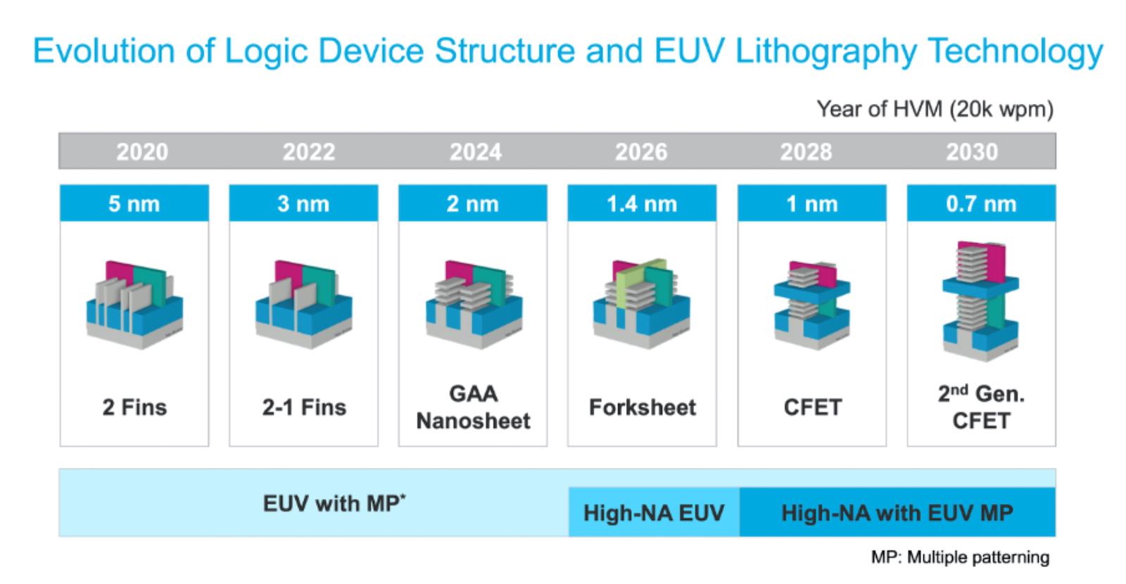
Source:
5nm (nanometer) is already in mass production at TSMC and Samsung while Intel is also working on it. Samsung and TSMC are starting production at 3nm and planning to introduce 2nm in 2025. Both are targeting 1.4nm after that. All three companies are aiming for 1nm and eventually smaller.
This cannot be done efficiently without the extreme ultraviolet (EUV) lithography tools now monopolized by the Netherlands' ASML. China's SMIC foundry is reportedly capable of 7nm and perhaps 5nm production using previous generation deep ultraviolet (DUV) lithography in a much more complicated process, but it will not be able to compete internationally as long as US sanctions prevent it from acquiring EUV machines.
Multiple patterning, which overcomes the wavelength limitations of lithography equipment, requires advanced etching equipment from TEL, Applied Materials or Lam Research. Advanced , other materials and equipment (some of it made by TEL, most of it made by Japanese, American and European companies) will also be required to reach 1nm.
The logic device structures shown in the diagram provide a sense of the complexity of the technology. The fins on a FinFET (fin field-effect transistor) refer to the shape of the source and drain regions of the device. FinFET devices have faster switching times and higher electric current density than planar semiconductor devices.
Gate-All-Around (GAA) transistors, as explained by ,“are a modified transistor structure where the gate contacts the channel from all sides and enables continued scaling,” beyond the limits of FinFET.
“Early GAA devices will use vertically-stacked nanosheets… The nanosheet dimensions can be scaled so that transistors can be sized for the specific performance required… GAA transistors will be the successors to FinFETs, with nanosheets evolving to nanowires. These GAA structures should carry through the advanced process nodes currently on the roadmap.”
Forksheet and CFET refer to more advanced forms of GAA designed for further scaling and performance gains.
High-numerical aperture (NA) EUV lithography, in the words of ASML,“is an evolutionary step in EUV technology and includes a novel optics design and significantly faster reticle and wafer stages… to enable higher-resolution patterning for even smaller transistor features.
“The numerical aperture of the system, combined with the wavelength used, determines the smallest printable feature… [It] has been designed to enable multiple future nodes beginning in 2025 as the industry's first deployment, followed by memory technologies at similar density.”

A cutaway overview of ASML's extreme ultraviolet (EUV) lithography equipment operation, as seen from above. Credit: ASML.
TEL, which dominates the market for photoresist processing equipment, is working with ASML to integrate its most advanced photoresist coater/developer with ASML's EUV lithography toward the aim of introducing high-NA EUV lithography for high-volume production by 2025. The work is being done at the imec-ASML joint high-NA EUV research laboratory in the Netherlands.
Imec, which stands for Interuniversity Microelectronics Center, is an international research and development organization headquartered in Belgium that brings leading semiconductor industry companies and academics together to advance chip technology.
It won't come cheap. TEL plans to spend 190 billion yen ($1.35 billion) on R&D this fiscal year (up from 158.2 yen billion last year) and to invest 75 billion yen in technology development and production facilities (up from 57.2 billion yen).
Over the next five years, the company now plans R&D spending of more than 1 trillion yen and capital spending of at least 400 billion yen.
TEL is in a strong financial position, with 485 billion yen in cash and equivalents at the end of September 2022, zero debt and depreciation approaching 50 billion yen per year. Nevertheless, the financial pressure is likely to be considerable as the downturn in the semiconductor industry intensifies.
Follow this writer on Twitter: @ScottFo83517667


Comments
No comment