Scanning Electron Microscope (SEM) Market To Grow By USD 1.08 Billion From 2024-2028, Driven By Focus On Nanotechnology And AI's Role In Market Transformation - Technavio
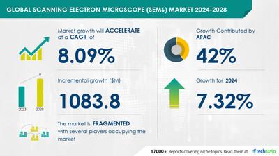
| Scanning Electron Microscope (SEMS) Market Scope |
|
| Report Coverage |
Details |
| Base year |
2023 |
| Historic period |
2018 - 2022 |
| Forecast period |
2024-2028 |
| Growth momentum & CAGR |
Accelerate at a CAGR of 8.09% |
| Market growth 2024-2028 |
USD 1083.8 million |
| Market structure |
Fragmented |
| YoY growth 2022-2023 (%) |
7.32 |
| Regional analysis |
APAC, North America, Europe, South America, and Middle East and Africa |
| Performing market contribution |
APAC at 42% |
| Key countries |
US, China, Japan, Germany, and South Korea |
| Key companies profiled |
Advantest Corp., Agilent Technologies Inc., Bruker Corp., Carl Zeiss Stiftung, COXEM Co. Ltd., Danaher Corp., DELONG INSTRUMENTS AS, Hirox Co. Ltd., Hitachi Ltd., HOVERLABS, JEOL Ltd., Keysight Technologies Inc., Nikon Corp., Nion, Olympus Corp., Seiko Holdings Corp., TESCAN GROUP, Thermo Fisher Scientific Inc., Tokyo Instruments Inc., and Topcon Corp. |
Market Driver
Scanning electron microscopes (SEMs) come in two main varieties: high-voltage electron microscopes (HVEMs) and low-voltage electron microscopes (LVEMs). While HVEMs operate at a high voltage of 100 kilovolts, LVEMs function at a reduced voltage of less than 25 kilovolts. This difference makes LVEMs more compact and cost-effective, allowing them to be used as tabletop or desktop microscopes. LVEMs are particularly suitable for specimens with a low atomic number, such as polymers , composite materials, pigments, minerals, cells, and membranes. These microscopes cause minimal damage to specimens due to lower radiation and offer high contrast. In contrast, HVEMs can damage specimens due to high radiation accumulation. LVEMs have gained popularity in life science, material science, pathology, and nanomaterial applications. Delong America is a leading vendor in this segment, offering products like LVEM5 and LVEM25, which function as both TEM and SEM. Although LVEMs are priced lower than conventional electron microscopes , they do not match their magnification capabilities. The increasing demand for LVEMs in various industries is expected to fuel the growth of the global scanning electron microscope market.
The Scanning Electron Microscope (SEM) market is experiencing significant growth due to increasing trends in nanotechnology and electronics. With the miniaturization of transistor chips and the demand for high resolution nanoscale imaging, SEMs play a crucial role in surface morphology analysis and chemical composition identification. The market caters to various industries including electronics, life sciences, and material sciences. Nanotechnology applications in areas like nanofibers, nanotubes, temperature superconductors, and alloy strength are driving the demand for SEMs. However, high excise taxes and custom duties pose challenges for market expansion. SEMs are used for failure analysis, drug development, material characterization, and correlative microscopy techniques like light microscopy and atomic force microscopy. Industries like aerospace, defense, and medical devices also rely on SEMs for quality control and clinical trials. Advancements in detector technology and the introduction of compact, high vacuum, low vacuum, cryo-SEM, environmental SEM, field emission SEM, tabletop SEM, dual-beam SEM, and other models continue to boost market growth.
Request Sample
of our comprehensive report now to stay ahead in the AI-driven market evolution!
Market
Challenges
-
The Scanning Electron Microscope (SEM) market is currently experiencing a challenge due to the high cost of SEMs, which is limiting demand. SEMs range in price from USD100,000 to USD1,250,000, with non-analytical models costing approximately USD700,000. Most vendors sell SEMs in this price range, while analytical models cost between USD400,000 and USD620,000. The price depends on the model's specifications and accessories. Organizations face budget constraints, making it difficult to purchase SEMs. Educational institutions and research organizations, which are significant buyers, depend on external funding, leading to uncertain sales. The high cost also impacts overseas sales due to customs taxes, which can reach up to 30% of the product cost. Potential customers often opt for renting SEMs instead, affecting new product sales. The price difference between new and used SEMs can be significant, reaching up to 50% or more. Consequently, the high cost of SEMs is expected to restrict market growth during the forecast period.
The Scanning Electron Microscope (SEM) market is experiencing significant growth due to its applications in various industries. Nanotechnology is a key driver, with SEMs used to examine nanofibers, nanotubes, and other nanoscale structures in materials science and biology. Chronic diseases and drug development also benefit from SEMs' high-resolution imaging capabilities. In industries like aerospace, defense, and environmental science, SEMs are used for material characterization and failure analysis. SEMs are also essential in research institutions for studying temperature superconductors, alloy strength, and other advanced materials. With the increasing demand for user-friendly software, compact models, and correlative microscopy techniques, SEMs are becoming more accessible to a wider range of users. New technologies like Cryo-SEM, Low vacuum SEM, and Field emission SEM are expanding the applications of SEMs, while automated features and intelligent technology enhance their efficiency. SEMs are also used in forensics and semiconductor manufacturing for specimen analysis and high-energy beam applications. Overall, the SEM market is poised for continued growth in various industries due to its versatility and importance in material science, nanotechnology, and research and development.
Discover how AI is revolutionizing market trends-
Get your access now!
Segment Overview
This scanning electron microscope (sems) market report extensively covers market segmentation by
Type-
1.1 Tabletop
1.2 Conventional
-
2.1 Semiconductor
2.2 Life sciences
2.3 Material sciences
2.4 Nanotechnology
-
3.1 APAC
3.2 North America
3.3 Europe
3.4 South America
3.5 Middle East and Africa
1.1
Tabletop- The tabletop segment of the global scanning electron microscope (SEM) market refers to compact and portable SEM systems designed for easy installation and use in laboratories and educational institutions. Their smaller size and affordability make tabletop SEMs an accessible and cost-effective option for researchers and educators in small facilities. These systems offer high-resolution imaging capabilities with efficient data acquisition, enabling quick analysis and increased productivity. Tabletop SEMs cater to various applications in materials science, nanotechnology, life sciences, and more, expanding their value to researchers and institutions. With user-friendly interfaces and simplified operations, these systems are suitable for users of all experience levels. Their maintenance requirements are also less complex compared to larger SEM systems, reducing operational downtime and costs. These factors are expected to fuel the growth of the tabletop segment in the global SEM market.
Download a Sample
of our comprehensive report today to discover how AI-driven innovations are reshaping competitive dynamics
Research Analysis
The Scanning Electron Microscope (SEM) market encompasses nanotechnology applications in various industries, including the semiconductor industry, electronics, and materials science. SEMs utilize electron beams to achieve high-resolution imaging at the nanoscale, revealing surface morphology, chemical analysis, fractography, and other critical details. These microscopes are essential for nanoscale imaging and analysis in sectors such as nanotechnology, nanoscale materials, and medical research. SEMs offer magnification capabilities far beyond light microscopy, enabling the examination of high-energy beam-sensitive specimens and nanoscale structures. They are indispensable tools for semiconductor wafer analysis, materials science, and biology. Correlative microscopy techniques, such as SEM-Atomic Force Microscopy (AFM), further expand their capabilities. Detector technology advancements continue to improve resolution power, making SEMs an intelligent technology for high-precision analysis and research.
Market Research Overview
The Scanning Electron Microscope (SEM) market encompasses various industries, including nanotechnology, electronics, life sciences, material sciences, and more. SEMs utilize electron beams to achieve high-resolution imaging of nanoscale structures, providing valuable information on surface morphology, chemical analysis, fractography, and more. Applications span from nanofibers and nanotubes in material sciences to temperature superconductors and alloy strength in aerospace and defense. SEMs are essential for miniaturization in electronics, such as transistor chips, and for quality control in manufacturing processes. Sample preparation is a critical aspect of SEM analysis, with various techniques employed to ensure accurate results. High excise taxes and custom duties pose challenges to the market, particularly for research institutions and smaller businesses. Advanced detector technology, user-friendly software, and automated features are driving the development of compact SEMs and other innovative SEM models, including high vacuum, low vacuum, cryo-SEM, environmental SEM, field emission SEM, tabletop SEM, dual-beam SEM, and more. SEMs play a crucial role in failure analysis, drug development, material characterization, and various fields, including biology, correlative microscopy techniques, and forensics. Intelligent technology and automated features are enhancing the capabilities of SEMs, enabling new applications in nanotechnology, medical research, and semiconductor wafers . High-energy beam magnification and specimen analysis are key features that enable SEMs to provide valuable insights into nanoscale materials and structures.
Table of Contents:
1 Executive Summary
2 Market Landscape
3 Market Sizing
4 Historic Market Size
5 Five Forces Analysis
6 Market Segmentation
-
Type
-
Tabletop
Conventional
-
Semiconductor
Life Sciences
Material Sciences
Nanotechnology
-
APAC
North America
Europe
South America
Middle East And Africa
7 Customer Landscape
8 Geographic Landscape
9 Drivers, Challenges, and Trends
10 Company Landscape
11 Company Analysis
12 Appendix
About Technavio
Technavio is a leading global technology research and advisory company. Their research and analysis focuses on emerging market trends and provides actionable insights to help businesses identify market opportunities and develop effective strategies to optimize their market positions.
With over 500 specialized analysts, Technavio's report library consists of more than 17,000 reports and counting, covering 800 technologies, spanning across 50 countries. Their client base consists of enterprises of all sizes, including more than 100 Fortune 500 companies. This growing client base relies on Technavio's comprehensive coverage, extensive research, and actionable market insights to identify opportunities in existing and potential markets and assess their competitive positions within changing market scenarios.
Contacts
Technavio Research
Jesse Maida
Media & Marketing Executive
US: +1 844 364 1100
UK: +44 203 893 3200
Email:
[email protected]
Website:
SOURCE Technavio
WANT YOUR COMPANY'S NEWS FEATURED ON PRNEWSWIRE? 440k+Newsrooms &
Influencers 9k+
Digital Media
Outlets 270k+
Journalists
Opted In GET STARTED

Legal Disclaimer:
MENAFN provides the
information “as is” without warranty of any kind. We do not accept
any responsibility or liability for the accuracy, content, images,
videos, licenses, completeness, legality, or reliability of the information
contained in this article. If you have any complaints or copyright
issues related to this article, kindly contact the provider above.


Comments
No comment