(MENAFN- Asia Times) Huawei and Chinese Electronic Design Automation (EDA) companies have reportedly developed an integrated circuit (IC) design automation platform for producing semiconductors with features as small as 14 nanometers (nm).
Evaluation and testing of the technology should be completed this year, according to a Chinese media report. Asia Times could not independently confirm the report.
If and when the testing and evaluation are successfully completed, China will have likely taken a big step toward overcoming progressively punitive US government sanctions on its semiconductor industry.
14nm is the most advanced process node used by SMIC, which runs China's largest semiconductor foundry. The new EDA tools should cover most of the chips China needs for industrial, automotive and consumer applications.
The new EDA tools, if as viable as reported, could also cause headaches for EDA industry leaders Synopsys, Cadence Design Systems and Siemens EDA (formerly Mentor Graphics), all of which are based in the US and subject to US government export restrictions to China.
Those restrictions currently affect only their most advanced technology, namely software used to design gate-all-around transistors starting at 3nm, but given the increasingly hostile attitude in Washington towards China, why should the Chinese take any chances? And why would the Chinese develop their own EDA tools and then not use them as maximally?
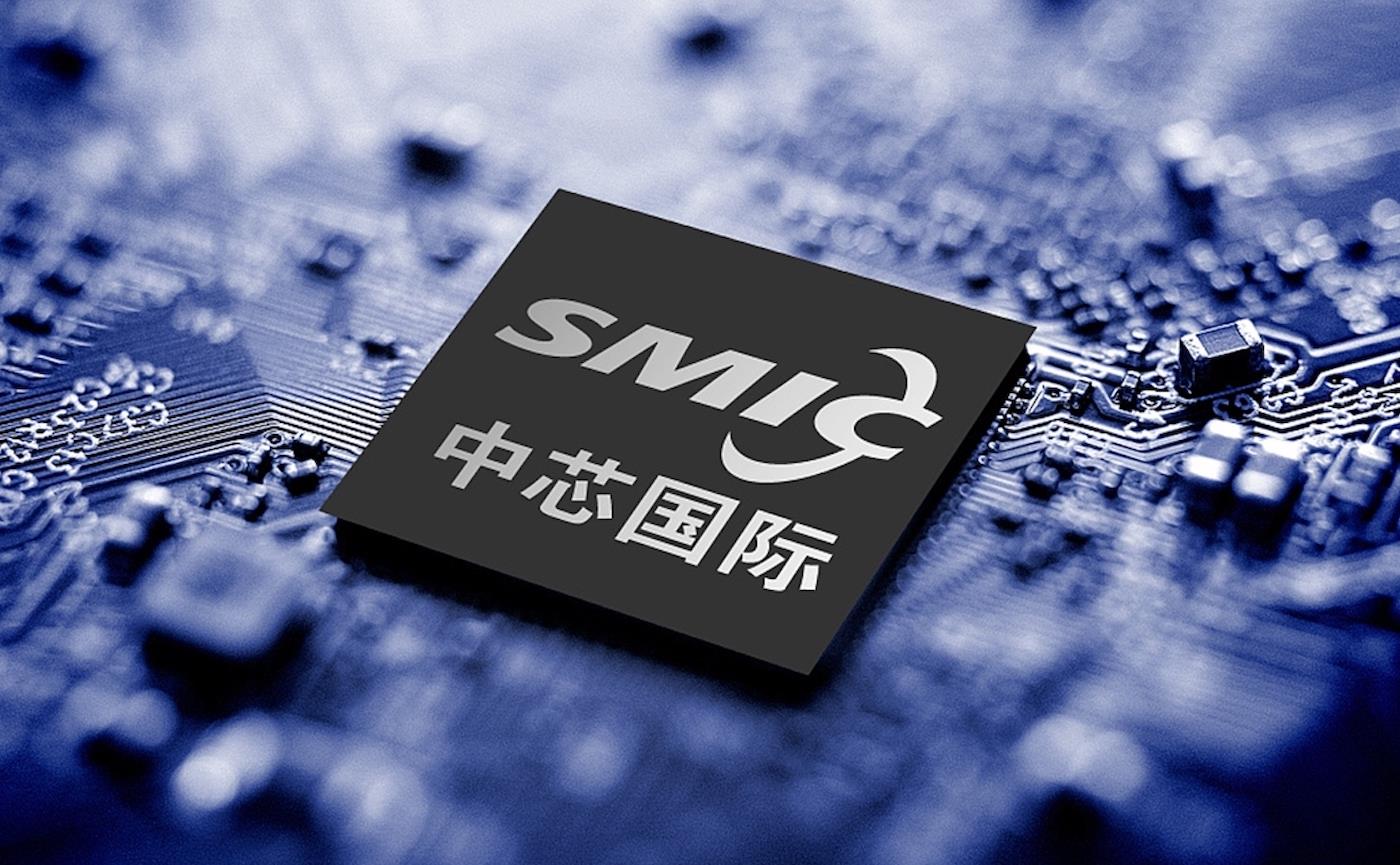
China's SMIC chipmaker is working to transcend US sanctions. Image: Twitter / Global Times
Cadence and Synopsis have recently made about 15% of their sales in China. Both companies' total sales are growing at high double-digit rates. However, Synopsys' guidance for investors this fiscal year assumes no further changes to US government export controls while Cadence notes the possibility of significant changes in its geographic earnings mix.
Mentor Graphics was delisted in 2017 after being acquired by Siemens. Now part of the company's Digital Industries division, Siemens EDA appears to be growing in line with its two main competitors. The three companies together account for about 75% of worldwide EDA industry revenues.
In addition to Huawei, Chinese companies working on EDA include Empyrean Technology, X-Epic, Cellixsoft, Xpedic and others. Empyrean, which
provides analog and mixed-signal IC, SoC (system-on-chip) and flat panel display (FPD) design solutions, is the most advanced but the others should not be written off.
According to a report in Digitimes, eight of 23 EDA companies working with Samsung Foundry are Chinese, a perch they have achieved through their technology and competitive pricing. American fears of the Chinese driving down prices to take market share are starting to be realized, probably sooner than they otherwise would be due to sanctions.
The next target for China's EDA industry will be 7nm, which is currently the limit of the country's lithography capability. The barriers to entry at smaller nodes rise steeply because exports of EUV lithography equipment to China are banned and exports of DUV equipment are likely to be restricted within the next few months.
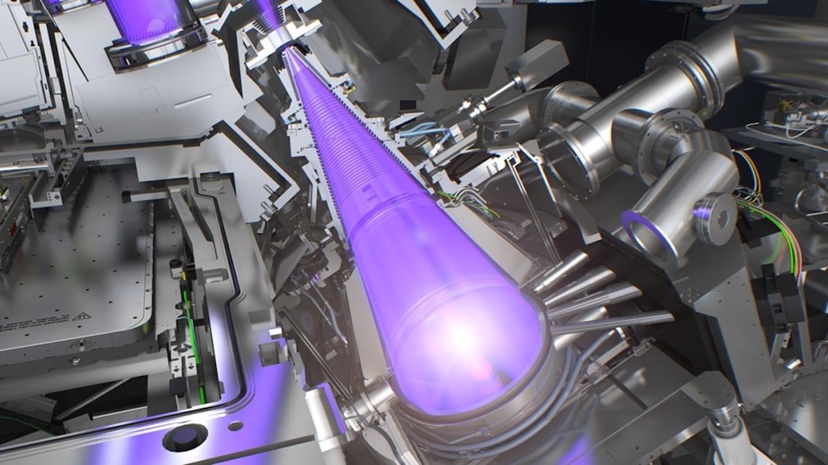
Light and lasers are key to THE Netherlands' ASML's lithography equipment. Photo: ASML
At the same time, semiconductor design and related lithography technology are advancing rapidly at the leading edge. Last October, Taiwanese high-tech research organization TrendForce wrote that if current trends continue,
“...it will not be difficult for China to realize semiconductor autonomy in processes above 10nm,” and
“Domestic Chinese IC designers who are committed to the development of SoCs, cloud computing chips, and GPUs are destined to move to more advanced manufacturing processes in order to meet the iterative needs of product upgrades and are expected to move toward the 4nm manufacturing process in the next 2 to 4 years,”
But the impact of US restrictions on EDA software“is expected to gradually emerge in 2025, not only delaying the development schedule of some domestic Chinese IC designers but even causing developmental stagnation.”
With the announcement of Huawei's 14nm EDA platform, this forecast points straight at the next battleground.
On March 21, Nvidia, the world's leading designer of graphics processing units (GPUs), announced a new software library called cuLitho that brings accelerated computing to computational semiconductor lithography.
CuLitho should speed up the production of photomasks by three to five times using a fraction of the power required by current solutions. It should result in better design rules, higher density and higher yields as chip makers move to 2nm and below.
The technology was developed over four years in collaboration with Synopsys (the world's largest EDA company), ASML (the monopoly producer of EUV lithography equipment) and TSMC (the world's leading IC foundry). TSMC plans to qualify it for production starting in June.
For a detailed presentation of CuLitho's potential, watch Nvidia CEO Jensen Huang's keynote speech at the company's GPU Technology Conference held on March 21 (starting at 22 minutes and 33 seconds).
A software library, as defined by Techopedia, is a suite of data and programming code used to develop software programs and applications. Photolithography is the process by which IC designs are created on silicon wafers. Photomasks are the design templates.
ASML explains computational lithography as follows:
“During lithography, diffraction of the light as well as physical and chemical effects in the photosensitive layer [on the wafer] deform the image the machine is trying to print (think of this as trying to draw a thin fine line with a broad watercolor paint brush – it smudges in many places).
“Computational lithography uses algorithmic models of the manufacturing process, calibrated with key data from our machines and from test wafers... to optimize the scanner [lithography machine], masks and processes for device manufacturability and yield...
“Without computational lithography, it would be impossible for chipmakers to manufacture the latest technology nodes.”
Top executives involved in the development and application of cuLitho have this to say about the technology:
Jensen Huang, CEO of Nvidia:“With lithography at the limits of physics, NVIDIA's introduction of cuLitho and collaboration with our partners TSMC, ASML and Synopsys allows fabs to increase throughput, reduce their carbon footprint and set the foundation for 2nm and beyond.”
Dr C C Wei, CEO of TSMC:“The cuLitho team has made admirable progress on speeding up computational lithography by moving expensive operations to GPU. This development opens up new possibilities for TSMC to deploy lithography solutions like inverse lithography technology and deep learning more broadly in chip manufacturing, making important contributions to the continuation of semiconductor scaling.”
Peter Wennink, CEO of ASML:“We are planning to integrate support for GPUs into all of our computational lithography software products. Our collaboration with NVIDIA on GPUs and cuLitho should result in tremendous benefit to computational lithography, and therefore to semiconductor scaling. This will be especially true in the era of high NA extreme ultraviolet lithography.”
Aart de Geus, CEO of Synopsys:“Computational lithography, specifically optical proximity correction, or OPC, is pushing the boundaries of compute workloads for the most advanced chips. By collaborating with our partner NVIDIA to run Synopsys OPC software on the cuLitho platform, we massively accelerated the performance from weeks to days!”
Optical proximity correction compensates for errors caused by light diffraction or process effects in order to improve the accuracy of photolithography. ASML's high-NA EUV lithography systems are scheduled for high-volume production in 2025.
The Chinese are not likely to catch up with this technology anytime soon, but they will be inspired to try.
Follow this writer on
Twitter: @ScottFo83517667
Like this:Like Loading...




Comments
No comment