(MENAFN- Asia Times) South Korea's Samsung Electronics plans to establish a central research and development (R&D) facility and will likely build a semiconductor packaging test line in Japan, initiatives that come against the backdrop of a recent rapid improvement in bilateral ties and the ongoing US-driven“decoupling” of the global tech industry.
According to Japanese and Korean press reports, the world's top producer of memory chips and second-ranking integrated circuit (IC) foundry plans to unify its R&D effort at its Yokohama Research Institute under the name Device Solution Research Japan (DSRJ). Samsung Electronics previously maintained half a dozen research facilities in Japan.
As reported by Pulse, DSRJ will hire Japanese as well as Korean researchers, an arrangement that should facilitate more interchange with Japanese suppliers and customers.
Pulse quoted an unidentified Korean business official as saying,“In the past, there was a perception that we have nothing more to learn from Japan, but Japan is still at the forefront of advanced technology. Samsung Electronics' new integrated R&D center in Japan may signal the company's intention to restore its link with Japan.”
That is – or was – a popular sentiment in South Korea that had lots to do with historical resentment, but very little to do with commercial reality. Samsung and SK Hynix, South Korea's other large semiconductor maker, have long depended on Japanese equipment and materials suppliers – and vice versa.
Over the past five years, Tokyo Electron – Japan's largest and the world's third-biggest supplier of semiconductor production equipment – has made nearly 20% of its sales in South Korea.
Japanese makers of photoresists and other chemicals used in the semiconductor manufacturing process – products in which they have dominant global market shares – also have substantial business in South Korea.
This became a political issue in 2019, when the South Korean Supreme Court ruled that Japanese companies must compensate Koreans forced to work for them during World War II.
Japan responded with export restrictions , causing massive inconvenience and disruption for both Korean customers and Japanese suppliers. Those restrictions were lifted in March of this year on the occasion of South Korean President Yoon Suk Yeol's visit to Tokyo.
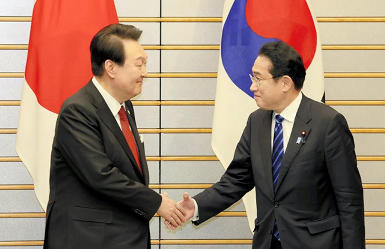
Prime Minister Fumio Kishida (R) shakes hands with South Korean President Yoon Suk Yeol (L) prior to the start of their meeting on March 16 at the Prime Minister's Official Residence. Image: Twitter
According to DigiTimes,“Samsung stated that this organizational restructuring [of R&D in Japan] has nothing to do with the improvement of governmental relations between South Korea and Japan.”
In other words, it was reportedly a business decision grounded firmly in the company's assessment of market conditions and opportunities.
In addition, Samsung is reportedly planning to build a test line for the development of new semiconductor packaging technology in Yokohama at a cost estimated at more than 30 billion yen (US$220 million).
This is an area in which Japanese equipment and material makers are particularly strong. Taiwan's TSMC, the world's leading IC foundry, opened a 3d ic packaging r&d center in Japan's Tsukuba Science City almost a year ago. More than 20 Japanese materials and equipment companies are working with TSMC in Tsukuba.
Construction of the packaging facility should start this year, according to press reports, with operation scheduled to begin in 2025. Several hundred people are likely to be employed. Like TSMC and US memory chip maker Micron before it, Samsung is expected to receive generous government subsidies to build semiconductor production facilities in Japan.
Samsung did not provide comments for the story but the amount of detail and the fact that it was front-page news in Japan suggests that there is something to it.
Last December, Samsung established an AVP (Advanced Package) Business Team within its Device Solutions Division. Working with its Japanese suppliers at a prototype development facility in Yokohama would be a logical next step.
If TSMC needs to be in Japan to get the most out of Japanese packaging technology, Samsung probably does as well. Samsung's foundry business is still only one-third the size of TSMC's.
This would be Samsung's first semiconductor production facility in Japan and a major step forward in the collaboration between the two countries' semiconductor industries. Sony is a customer of Samsung Foundry but production is done in Korea. TSMC, Sony and Toyota Group components maker Denso are building a semiconductor factory in kyushu , Japan.
Advanced packaging aims to overcome the physical limits of miniaturization – to go beyond Moore's Law, the prediction made in 1965 by Intel co-founder Gordon Moore that the density of transistors on an integrated circuit would continue to double roughly every two years.
In Samsung's words:
“Through advanced Heterogeneous Integration, which connects multiple chips horizontally and vertically, more transistors can be planted on a single chip (or package) and offer performance that is more powerful than the sum of all parts.”
“Our focus areas are the development of next-generation 2.5D and 3D advanced package solutions based on RDL,
Si Interposer/Bridge
and TSV
stacking technologies.”
These technical terms are defined as follows:
2.5D package: A package which integrates a single-layer logic semiconductor and multi-layer memory semiconductor together on a substrate.
3D package: a package in which multiple logic/memory semiconductors are vertically integrated.
RDL (Redistribution Layer): Advanced packaging technology that places an extra metal layer in between a small and large circuit board to integrate the two.
Si Interposer/Bridge: The microcircuit board inserted between the IC chip and PCB, which physically connects the chip and board by acting as the mid-level wiring.
TSV (Through Silicon Via): Advanced package technology that grinds the surface of the chip, drills hundreds of microscopic holes and connects the electrodes that vertically penetrate the holes in the top and bottom chips.
Samsung's advanced packaging also includes chiplets, which are“small, modular chips that can be combined to form a larger, more complex system-on-a-chip (SoC).
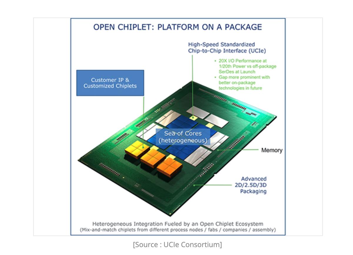
They offer a number of benefits over traditional monolithic chips, including improved performance, cost savings, and design flexibility,” according to industry information service anysilicon.
Along with die shrinks to 3nm and below, advanced packaging is the leading edge of semiconductor production technology.
South Korean President Yoon and Japanese Prime Minister Fumio Kishida are scheduled to meet during the G7 Summit in Hiroshima, scheduled to be held May 19-21. More information about Samsung's investments and other economic collaboration between South Korea and Japan may be announced at the event.
Follow this writer on
Twitter: @ScottFo83517667
Like this:Like Loading...


Comments
No comment